당신은 주제를 찾고 있습니까 “semiconductor physics and devices 4th edition – Introduction to Semiconductor Physics and Devices“? 다음 카테고리의 웹사이트 https://ro.taphoamini.com 에서 귀하의 모든 질문에 답변해 드립니다: https://ro.taphoamini.com/wiki. 바로 아래에서 답을 찾을 수 있습니다. 작성자 Jordan Edmunds 이(가) 작성한 기사에는 조회수 145,662회 및 좋아요 1,609개 개의 좋아요가 있습니다.
Table of Contents
semiconductor physics and devices 4th edition 주제에 대한 동영상 보기
여기에서 이 주제에 대한 비디오를 시청하십시오. 주의 깊게 살펴보고 읽고 있는 내용에 대한 피드백을 제공하세요!
d여기에서 Introduction to Semiconductor Physics and Devices – semiconductor physics and devices 4th edition 주제에 대한 세부정보를 참조하세요
https://www.patreon.com/edmundsj
If you want to see more of these videos, or would like to say thanks for this one, the best way you can do that is by becoming a patron – see the link above :). And a huge thank you to all my existing patrons – you make these videos possible.
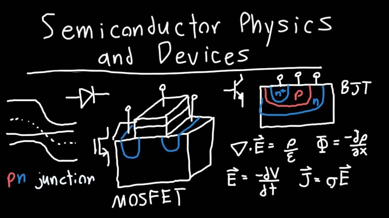
In this video, I talk about the roadmap to learning semiconductor physics, and what the driving questions we are trying to answer are.
This is part of my series on semiconductor physics (often called Electronics 1 at university). This is based on the book Semiconductor Physics and Devices by Donald Neamen, as well as the EECS 170A/174 courses taught at UC Irvine.
Hope you found this video helpful, please post in the comments below anything I can do to improve future videos, or suggestions you have for future videos.
semiconductor physics and devices 4th edition 주제에 대한 자세한 내용은 여기를 참조하세요.
Semiconductor Physics and Devices – OptiMa-UFAM
SEMICONDUCTOR PHYSICS & DEVICES: BASIC PRINCIPLES, FOURTH EDITION … Semiconductor physics and devices : basic principles / Donald A. Neamen. — 4th ed.
Source: www.optima.ufam.edu.br
Date Published: 10/18/2022
View: 7303
Physics of Semiconductor Devices, 4th Edition – Wiley
The Fourth Edition of Physics of Semiconductor Devices remains the standard reference work on the fundamental physics and operational characteristics of all …
Source: www.wiley.com
Date Published: 12/6/2021
View: 4487
Semiconductor Physics and Devices – Fulvio Frisone
Semiconductor physics and devices : basic principles 1 Donald A. Neamen. -3rd ed. p. cm. Includes bibliographical references and index. ISBN 0-07-232 107- …
Source: www.fulviofrisone.com
Date Published: 12/2/2022
View: 2703
Semiconductor Physics and Devices 4th edition Neaman pdf
Semiconductor Physics and Devices: Basic Principles, 4th edition Chapter 1. By D. A. Neamen Problem Solutions. ______. ______. Chapter 1. Problem Solutions.
Source: www.studocu.com
Date Published: 11/23/2022
View: 2444
Semiconductor Physics Devices Donald Neamen 4th Edition
Yeah, reviewing a book Semiconductor Physics Devices Donald Neamen 4th Edition could be credited with your near associates listings.
Source: tunxis.commnet.edu
Date Published: 7/21/2021
View: 6650
주제와 관련된 이미지 semiconductor physics and devices 4th edition
주제와 관련된 더 많은 사진을 참조하십시오 Introduction to Semiconductor Physics and Devices. 댓글에서 더 많은 관련 이미지를 보거나 필요한 경우 더 많은 관련 기사를 볼 수 있습니다.
주제에 대한 기사 평가 semiconductor physics and devices 4th edition
- Author: Jordan Edmunds
- Views: 조회수 145,662회
- Likes: 좋아요 1,609개
- Date Published: 2018. 3. 25.
- Video Url link: https://www.youtube.com/watch?v=OVnVN0vSXn0
Physics of Semiconductor Devices, 4th Edition
S. M. SZE, P H D, is Honorary Chair Professor, College of Electrical and Computer Engineering, National Chiao Tung University, Taiwan. He has made fundamental and pioneering contributions to semiconductor devices, particularly his co-discovery of the floating-gate memory (FGM) effect that has ushered in the Fourth Industrial Revolution. Dr. Sze has authored, co-authored, and edited more than 400 papers and 16 books. He is a celebrated Member of IEEE, an Academician of Academia Simica, and a member of the US National Academy of Engineering.
YIMING LI, P H D, is Full Professor of Electrical and Computer Engineering at National Chiao Tung University, Taiwan. He has been a Visiting Professor in Stanford University, Grenoble INP, and Tohoku University. He has published more than 300 technical articles in journals, conferences, and book chapters. Dr. Li is an active member of IEEE and has served on technical committees for many international professional conferences including IEDM. He is the recipient of the Pan Wen-Yuan Foundation’s Research Fellowship Award and the Chinese Institute of Electrical Engineering’s Outstanding Young Electrical Engineer Award.
Semiconductor Physics and Devices 4th edition Neaman pdf
Semiconductor Physics and Devices: Basic Principles, 4 edition Chapter 1
By D. A. Neamen Problem Solutions
Chapter 1
Problem Solutions
1.
(a) fcc: 8 corner atoms 8/1 1 atom
6 face atoms 2/1 3 atoms
Total of 4 atoms per unit cell
(b) bcc: 8 corner atoms 8/1 1 atom
1 enclosed atom =1 atom Total of 2 atoms per unit cell
(c) Diamond: 8 corner atoms 8/1 1 atom
6 face atoms 2/1 3 atoms
4 enclosed atoms = 4 atoms Total of 8 atoms per unit cell
1.
(a) Simple cubic lattice: a 2 r
Unit cell vol
3 3 3 a 2 r 8 r
1 atom per cell, so atom vol
3
4 1
3 r
Then
Ratio 100 % 52 %4. 8
3
4
3
3
r
r
(b) Face-centered cubic lattice
r
d d r a a 2 2 2
4 2
Unit cell vol
3 3 3 a 2 2 r 16 2 r
4 atoms per cell, so atom vol
3
4 4
3 r
Then
Ratio
100 % 74 % 16 2
3
4 4
3
3
r
r
(c) Body-centered cubic lattice
d r a a r 3
4 43
Unit cell vol
3 3
3
4
a r
2 atoms per cell, so atom vol
3
4 2
3 r
Then
Ratio
100 % 68 %
3
4
3
4 2
3
3
r
r
(d) Diamond lattice
Body diagonal d r a a r 3
8 8 3
Unit cell vol
3 3
3
8
r a
8 atoms per cell, so atom vol
3
4 8
3 r
Then
Ratio
100 % 34 %
3
8
3
4 8
3
3
r
r
1.
(a)
o a .5 43 A ; From Problem 1,
a r 3
8
Then
o
A
a r .1 176 8
.5 43 3
8
3
Center of one silicon atom to center of
nearest neighbor
o 2 r .2 35 A (b) Number density
22 83
5 10 .5 43 10
8
cm 3
(c) Mass density
23
22
.6 02 10
.. 5 10 28. 09
NA
NAtWt
.2 33 grams/cm 3
Semiconductor Physics and Devices: Basic Principles, 4 edition Chapter 1
By D. A. Neamen Problem Solutions
1.
(a) 4 Ga atoms per unit cell
Number density
83 .5 65 10
4
Density of Ga atoms 22 .2 22 10 cm 3
4 As atoms per unit cell
Density of As atoms
22 .2 22 10 cm 3
(b) 8 Ge atoms per unit cell
Number density
83 .5 65 10
8
Density of Ge atoms 22 .4 44 10 cm 3
1.
From Figure 1.
####### (a) a
a d .0 4330 2
3
2
o .0 4330 .5 65 d .2 447 A
(b) a
a d 2 .0 7071 2
o .0 7071 .5 65 d .3 995 A
1.
54. 74 3 2
2
3 2
2 2 2
sin
a
a
109 5.
1.
(a) Simple cubic:
o a 2 r 9 A
(b) fcc:
o A
r a .5 515 2
4
(c) bcc:
o A
r a .4 503 3
4
(d) diamond:
####### o
A
r a .9 007 3
42
1.
####### (a) .12 035 2 .12 035 2 rB
o rB .0 4287 A
(b)
o a .12 035 .2 07 A
(c) A-atoms: # of atoms 1 8
1 8
Density
83 .2 07 10
1
23 .1 13 10 cm 3
B-atoms: # of atoms 3 2
1 6
Density
83 .2 07 10
3
23 .3 38 10 cm 3
1.
(a)
o a 2 r 5 A
8
of atoms 1
1 8
Number density
83 5 10
1
22 .1 097 10 cm 3
Mass density
#######
NA
NAtWt ..
23
22
.6 02 10
.1 0974 10 12 5.
.0 228 gm/cm
3
(b)
o A
r a .5 196 3
4
8
of atoms 1 2
1 8
Number density
83 .5 196 10
2
22 .1 4257 10 cm
3
Mass density
23
22
.6 02 10
.1 4257 10 12 5.
.0 296 gm/cm
3
1. From Problem 1, percent volume of fcc atoms is 74%; Therefore after coffee is ground,
Volume = 0 cm 3
Semiconductor Physics and Devices: Basic Principles, 4 edition Chapter 1
By D. A. Neamen Problem Solutions
1.
(a)
313
1
1 , 3
1 , 1
1
(b)
121
4
1 , 2
1 , 4
1
1.
Intercepts: 2, 4, 3
3
1 , 4
1 , 2
1
(634) plane
1.
(a)
o d a .5 28 A
(b)
o A
a d .3 734 2
2
(c)
o A
a d .3 048 3
3
1.
(a) Simple cubic
(i) (100) plane:
Surface density
2 82 .4 73 10
1 1
a
14 .4 47 10 cm 2
(ii) (110) plane:
Surface density 2
1 2 a
14 .3 16 10 cm 2
(iii) (111) plane:
Area of plane bh 2
1
where
o b a 2 .6 689 A
Now
2
2 2 2 2 4
3
2
2 2 a
a h a
So
o h .4 73 .5 793 A 2
6
Area of plane
8 8 .6 68923 10 .5 79304 10 2
1
16 19. 3755 10
cm 2
Surface density 16 19. 3755 10
6
1 3
14 .2 58 10 cm 2
(b) bcc (i) (100) plane:
Surface density
14 2 .4 47 10
1 a
cm 2
(ii) (110) plane:
Surface density 2
2 2 a
14 .6 32 10 cm 2
(iii) (111) plane:
Surface density 16 19. 3755 10
6
1 3
14 .2 58 10 cm 2
(c) fcc (i) (100) plane:
Surface density
14 2 .8 94 10
2 a
cm 2
(ii) (110) plane:
Surface density 2
2 2 a
14 .6 32 10 cm 2
(iii) (111) plane:
Surface density 16 19. 3755 10
2
1 3 6
1 3
15 .1 03 10 cm 2
1. (a) (100) plane: – similar to a fcc:
Surface density
82 .5 43 10
2
14 .6 78 10 cm 2
(b) (110) plane:
Surface density
82 .52 43 10
4
14 .9 59 10 cm 2
Semiconductor Physics and Devices: Basic Principles, 4 edition Chapter 1
By D. A. Neamen Problem Solutions
(c) (111) plane:
Surface density
82 .523 43 10
2
14 .7 83 10 cm 2
1.
o
A
r a .6 703 2
.24 37
2
4
(a) #/cm 3
3 83 .6 703 10
2 4
1 6 8
1 8
a
22 .1 328 10 cm 3
(b) #/cm
2
2
2
1 2 4
1 4
2 a
.6 703 10 2
2 82
14 .3 148 10 cm 2
(c)
o
A
a d .4 74 2
.6 703 2
2
2
(d) # of atoms 2 2
1 3 6
1 3
Area of plane: (see Problem 1) o b a 2 .9 4786 A
o A
a h .8 2099 2
6
Area
8 8 .9 4786 10 .8 2099 10 2
1
2
1 bh
15 .3 8909 10 cm 2
#/cm 2 15 .3 8909 10
2
= 14 .5 14 10 cm 2
o
A
a d .3 87 3
.6 703 3
3
3
1.
Density of silicon atoms
22 5 10 cm 3 and
4 valence electrons per atom, so
Density of valence electrons 23 2 10 cm 3
1. Density of GaAs atoms
22 83
.4 44 10 .5 65 10
8
cm 3
An average of 4 valence electrons per atom, So Density of valence electrons 23 .1 77 10 cm 3
1.
(a) 100 % 10 % 5 10
5103 22
17
(b) 100 % 4 10 % 5 10
2106 22
15
1. (a) Fraction by weight
7 22
16 .1 542 10 5 10 28. 06
2 10 10. 82
(b) Fraction by weight
5 22
18 .2 208 10 5 10 28. 06
10 30. 98
1.
Volume density 16 3 2 10
1 d
cm 3
So 6 .3 684 10 d cm
o d 368 4. A
We have
o ao .5 43 A
Then 67. 85 .5 43
368 4. ao
d
1.
Volume density
15 3 4 10
1 d
cm
3
So
6 .6 30 10
d cm
o d 630 A
We have
o ao .5 43 A
Then 116 .5 43
630 ao
d
Semiconductor Physics and Devices: Basic Principles, 4 edition Chapter 2
By D. A. Neamen Problem Solutions
(b)
27 19 .12 67 10 6.12 10
p
23 .2 532 10
kg-m/s
11 23
34 .2 62 10 .2 532 10
.6 62510
m
or
o .0 262 A
2.
.0 0259 .0 03885
2
3
2
3
Eavg kT eV
Now
pavg 2 mEavg
31 19 .92 11 10 .0 03885 6 10
or
25 .1 064 10 pavg kg-m/s
Now
9 25
34 .6 225 10 .1 064 10
.6 62510
p
h m
or o 62. 25 A
2.
p
p p
hc E h
Now
m
p E e e 2
2 and
2
2
1
e
e e
e
h
m
E
h p
Set Ep Ee and p 10 e
Then
2 2 10
2
1
2
1
p e p
h
m
h
m
hc
which yields
mc
h p 2
100
100
2 2 100
2 mc mc h
hc hc E E p
p
100
.92 11 10 3 10
31 82
15 .1 64 10 J 10. 25 keV
2.
(a) 10
34
85 10
.6 625 10
h p
26 .7 794 10
kg-m/s
4 31
26 .8 56 10 .9 11 10
.7 794 10
m
p m/s
or 6 .8 56 10 cm/s
2 31 42 .9 11 10 .8 56 10 2
1
2
1 E m
21 .3 33 10 J
or
2 19
21 .2 08 10 6 10
.3 33410
E eV
(b)
31 32 .9 11 10 8 10 2
1
E
23 .2 915 10
J
or 4 19
23 .1 82 10 6 10
.2 91510
E eV
31 3 .9 11 10 8 10 p m
27 .7 288 10 kg-m/s
8 27
35 .9 09 10 .7 288 10
.6 62510
p
h m
or
o 909 A
2.
(a)
10
34 8
1 10
.6 625 10 3 10
hc E h
15 .1 99 10 J
Now
19
15
6 10
.1 99 10
e
E E Ve V
4 V .1 24 10 V 12 4. kV
(b)
31 15 2 .92 11 10 .1 99 10
p mE
23 .6 02 10
kg-m/s Then
11 23
34 .1 10 10 .6 02 10
.6 62510
p
h m
or o .0 11 A
Semiconductor Physics and Devices: Basic Principles, 4 edition Chapter 2
By D. A. Neamen Problem Solutions
2.
6
34
10
.1 054 10
x
p
28 .1 054 10
kg-m/s
2.
(a) (i) xp
26 10
34 .8 783 10 12 10
.1 05410
p kg-m/s
(ii) p m
p
dp
d p dp
dE E
2
2
m
pp p m
p 2
2
Now p 2 mE
31 19 92 10 16 6 10
24 .2 147 10
kg-m/s
so
31
24 26
9 10
.2 1466 10 .8 783 10
E
19 .2 095 10
J
or .1 31 6 10
.2 095 10 19
19
E eV
(b) (i)
26 .8 783 10
p kg-m/s
(ii)
28 19 52 10 16 6 10
p
23 .5 06 10
kg-m/s
28
23 26
5 10
.5 06 10 .8 783 10
E
21 .8 888 10
J
or
2 19
21 .5 55 10 6 10
.8 88810
E eV
2.
32 2
34 .1 054 10 10
.1 05410
x
p
kg-m/s
1500
.1 054 10
32
m
p p m
36 7 10 m/s
2. (a) tE
16 19
34 .8 23 10 6.18 10
.1 05410
t s
(b) 10
34
5 10
.1 054 10
x
p
25 .7 03 10 kg-m/s
2.
####### (a) If 1 , tx and 2 , tx are solutions to
Schrodinger’s wave equation, then
t
tx xV tx j x
tx
m
, ,
,
2
1 2 1
1
2 2
and
t
tx xV tx j x
tx
m
, ,
,
2
2 2 2
2
2 2
Adding the two equations, we obtain
tx tx
m x
, , 2 2 1 2
2 2
xV 1 , tx 2 , tx
tx tx
t
j 1 , 2 ,
which is Schrodinger’s wave equation. So
####### 1 , tx 2 , tx is also a solution.
####### (b) If 1 , tx 2 , tx were a solution to
Schrodinger’s wave equation, then we could write
1 2 1 2
2
2 2
2
xV m x
1 2
t
j
which can be written as
m x x x x
1 2 2
1
2
2 2
2
2
1
2 2 2
t t
xV j 1 2
2 1 2 1
Dividing by 1 2 , we find
m x x x x
1 2
21
2
1
2
1
2
2
2
2
2 1 1 2
2
t t
xV j 1
1
2
2
1 1
Semiconductor Physics and Devices: Basic Principles, 4 edition Chapter 2
By D. A. Neamen Problem Solutions
2.
####### P x dx
2
(a) dx
x
a
a
2
cos
22
4/
4/
40
2 sin
2
2
a
a
a
x
x
a
a
a
a
4
2
sin
2
2 4
4
1
8
2 a a
a
or P .0 409
(b) dx a
x
a
P
a
a
2/
4/
2 cos
2
2/
4 4/
2 sin
2
2
a
a a
a
x
x
a
a
a
a
a
a
4
2
sin
4 8
sin
4
2
4
1
8
1 0 4
1 2
or P .0 0908
(c) dx a
x
a
P
a
a
2
2/
2/
cos
2
2/
2/
4
2 sin
2
2
a
a a
a
x
x
a
a
a
a
a
a
4
sin
4 4
sin
4
2
or P 1
2.
(a) dx a
x
a
P
a
2 sin
22
4/
4/
2 4
4 sin
2
2
a
a
a
x
x
a
a
a
a
8
sin
8
2
or P .0 25
(b) dx a
x
a
P
a
a
2 sin
22
2/
4/
2/
4/
2 4
4 sin
2
2
a
a a
a
x
x
a
a
a
a
a
a
8
sin
8 8
sin 2
4
2
or P .0 25
(c) dx a
x
a
P
a
a
2 sin
22
2/
2/
2/
2/
2 4
4 sin
2
2
a
a a
a
x
x
a
a
a
a
a
a
8
sin 2
8 4
sin 2
4
2
or P 1
2.
(a) (i) 4 8
12 10 8 10
8 10
k
p
m/s
or 6 p 10 cm/s
9 8 .7 854 10 8 10
22
k
m
Semiconductor Physics and Devices: Basic Principles, 4 edition Chapter 2
By D. A. Neamen Problem Solutions
or
o 78. 54 A
(ii)
31 4 .9 11 10 10
p m 27 .9 11 10 kg-m/s
2 31 42 .9 11 10 10 2
1
2
1 E m
23 .4 555 10 J
or 4 19
23 .2 85 10 6 10
.4 55510
E eV
(b) (i) 4 9
13 10 5 10
5 10
k
p
m/s
or
6 p 10 cm/s
9 9 .4 19 10 5 10
22
k
m
or
o 41 9. A
(ii)
27 .9 11 10
p kg-m/s 4 .2 85 10
E eV
2.
(a)
j kx t tx Ae ,
(b)
19 2 2
1 E .0 025 6 10 m
31 2 .9 11 10 2
1
so
4 .9 37 10 m/s 6 .9 37 10 cm/s
For electron traveling in x direction, 6 .9 37 10 cm/s
31 4 .9 11 10 .9 37 10 p m
26 .8 537 10 kg-m/s
9 26
34 .7 76 10 .8 537 10
.6 62510
p
h m
8 9 .8 097 10 .7 76 10
2 2
k m 1
8 4 k .8 097 10 .9 37 10
or 13 .7 586 10 rad/s
2.
(a)
31 4 .9 11 10 5 10
p m 26 .4 555 10
kg-m/s
8 26
34 .1 454 10 .4 555 10
.6 62510
p
h m
8 8 .4 32 10 .1 454 10
2 2
k m 1
8 4 k .4 32 10 5 10 13 .2 16 10 rad/s
(b)
31 6 .9 11 10 10
p 25 .9 11 10 kg-m/s
10 25
34 .7 27 10 .9 11 10
.6 62510
m
9 10 .8 64 10 .7 272 10
2
k m 1
9 6 15 .8 64 10 10 .8 64 10 rad/s
2.
31 102
2 342 2
2
222
.92 11 10 75 10
.1 054 10
2
n
ma
n En
2 21 .1 0698 10 En n J
or
19
2 21
6 10
.1 0698 10
n En
or
2 3 .6 686 10
En n eV
Then 3 1 .6 6910
E eV 2 2 .2 6710
E eV 2 3 .6 0210
E eV
2.
(a)
31 102
2 342 2
2
222
.92 11 10 10 10
.1 054 10
2
n
ma
n En
2 20 .6 018 10 n J
or
.0 3761
6 10
.6 018102 19
2 20 n
n En
eV
Then E 1 .0 376 eV
E 2 .1 504 eV
E 3 .3 385 eV
(b) E
hc
19 .3 385 .1 504 6 10
E 19 .3 01 10
J
Semiconductor Physics and Devices: Basic Principles, 4 edition Chapter 2
By D. A. Neamen Problem Solutions
2
2
2
2
2
2
z
Z XY y
Y XZ x
X YZ
2 2 XYZ
mE
Dividing by XYZ and letting 2
2 2
mE k , we
find
(1) 0
1112 2
2
2
2
2
2
k z
Z
y Z
Y
x Y
X
X
We may set
12 2
2 2 2
2
k X x
X k x
X
X
x x
Solution is of the form
####### xX A sin xxk B cos xxk
####### Boundary conditions: X 0 0 B 0
####### and
a
n xX a k
x x
0
where nx …,2,
Similarly, let
2 2
2 1 ky y
Y
Y
and
2 2
2 1 kz z
Z
Z
Applying the boundary conditions, we find
a
n k
y y
, ny …,2,
a
n k
z z
, nz 3,2, …
From Equation (1) above, we have
2 2 2 2 kx ky kz k
or
2
2 2 2 2 2
mE kx ky kz k
so that
2 2 2 2
22
2
nnn nx ny nz ma
E E zyx
2.
(a)
, 0
, , 2 2 2
2
2
2
yx
mE
y
yx
x
yx
Solution is of the form:
, yx A sin xxk sin yyk
We find
#######
Ak xk yk x
yx x cos x sin y
,
Ak xk yk x
yx x sin x sin y
, 2 2
2
#######
Ak xk yk y
yx y sin x cos y
,
Ak xk yk y
yx y sin x sin y
, 2 2
2
Substituting into the original equation, we find:
(1) 0
2 2
2 2
mE kx ky
From the boundary conditions,
A sin xak 0 , where
o a 40 A
So a
n k
x x
, nx …,3,2,
Also A sin ybk 0 , where
o b 20 A
So b
n k
y y
, ny …,3,2,
Substituting into Eq. (1) above
2
22
2
2 22
2 b
n
a
n
m
E x y nn yx
(b)Energy is quantized – similar to 1-D result. There can be more than one quantum state per given energy – different than 1-D result.
2. (a) Derivation of energy levels exactly the same as in the text
(b)
2 1
2 2 2
22
2
n n ma
E
For n 2 ,2 n 1 1
Then
2
22
2
3
ma
E
(i) For
o a 4 A
27 102
342 2
.12 67 10 4 10
.13 054 10
E
22 .6 155 10
J
or
3 19
22 .3 85 10 6 10
.6 15510
E eV
Semiconductor Physics and Devices: Basic Principles, 4 edition Chapter 2
By D. A. Neamen Problem Solutions
(ii) For a 5 cm
27 22
34 2 2
.12 67 10 5 10
.13 054 10
E
36 .3 939 10
J or
17 19
36 .2 46 10 6 10
.3 93910
E eV
2.
(a) For region II, x 0
0
2 2 2 2
2
2
E V x
m
x
x O
General form of the solution is
####### 2 x A 2 exp jk 2 x B 2 exp jk 2 x
where
E VO
m k 22
2
Term with B 2 represents incident wave and
term with A 2 represents reflected wave.
Region I, x 0
0
2 2 2 1
1
2
x
mE
x
x
General form of the solution is
####### 1 x A 1 exp jk 1 x B 1 exp jk 1 x
where
12
2
mE k
Term involving B 1 represents the
transmitted wave and the term involving A 1
represents reflected wave: but if a particle is transmitted into region I, it will not be reflected so that A 1 0.
Then
####### 1 x B 1 exp jk 1 x
####### 2 x A 2 exp jk 2 x B 2 exp jk 2 x
(b) Boundary conditions:
####### (1) 1 x 0 2 x 0
(2) 0
2
1
x x x x
Applying the boundary conditions to the
solutions, we find
B 1 A 2 B 2
Ak 22 Bk 22 Bk 11
Combining these two equations, we find
2 2 1
2 1 2 B k k
k k A
2 2 1
2 1
2 B k k
k B
The reflection coefficient is 2
2 1
2 1 * 22
22
k k
k k
BB
AA R
The transmission coefficient is
2 1 2
421 1 k k
kk T R T
2.
####### 2 x A 2 exp 2 xk
xk
AA
x P 2 * 22
2
exp 2
where
#######
22
2
Vm E k o
34
31 19
.1 054 10
.92 11 10 5 6.18 10
9 k 2 .4 286 10 m 1
(a) For 10 5 5 10
o x A m
####### P exp 2 2 xk
9 10 exp .42 2859 10 5 10
.0 0138
(b) For 10 15 15 10
o x A m
9 10 exp .42 2859 10 15 10 P
6 .2 61 10
(c) For 10 40 40 10
o x A m
9 10 exp .42 2859 10 40 10 P
15 .1 29 10
2.
ak
V
E
V
E T o o
161 exp 22
where
#######
22
2
Vm E k
o
34
31 19
.1 054 10
.92 11 10 0 6.11 10
Semiconductor Physics and Devices: Basic Principles, 4 edition Chapter 2
By D. A. Neamen Problem Solutions
where
12
2
mE k
Region II:
####### 2 x A 2 exp 2 xk B 2 exp 2 xk
where
22
2
Vm E k
O
Region III:
####### 3 x A 3 exp jk 1 x B 3 exp jk 1 x
(b)
In Region III, the B 3 term represents a
reflected wave. However, once a particle is transmitted into Region III, there will
not be a reflected wave so that B 3 0.
(c) Boundary conditions: At x 0 : 1 2
A 1 B 1 A 2 B 2
dx
d
dx
d 1 2
jkA 11 jkB 11 Ak 22 Bk 22
At x a : 2 3
####### A 2 exp 2 ak B 2 exp 2 ak
####### A 3 exp jk 1 a
dx
d
dx
d 2 3
####### Ak 22 exp 2 ak Bk 22 exp 2 ak
####### jkA 31 exp jk 1 a
The transmission coefficient is defined as
11
33
AA
AA T
so from the boundary conditions, we want to solve for A 3 in terms of A 1. Solving
for A 1 in terms of A 3 , we find
k k ak ak
kk
jA A 2 2 2 1
2 2 21
3 1 exp exp 4
2 jkk 21 exp 2 ak exp 2 ak
####### exp jk 1 a
We then find
k k ak
kk
AA AA 2
2 1
2 2 2 21
33 11 exp 4
2 exp 2 ak
2 2 2
2 2
2 41 kk exp ak exp ak
We have
#######
22
2
Vm E k O
If we assume that VO E , then 2 ak will
be large so that
####### exp 2 ak exp 2 ak
We can then write
2 2
2 1
2 2 2 21
33 11 exp 4
k k ak kk
AA AA
2 2
2 2
2 41 kk exp ak
which becomes
k k ak
kk
AA AA 2
2 1
2 2 2 21
33 11 exp 2 4
Substituting the expressions for k 1 and
k 2 , we find
2
2 2
2 1
2
mVO k k
and
2 2
2 2
2 1
22
Vm E mE kk O
V E E
m O
2
2
2
E
V
E V
m
O
O
1
2
2
2
Then
E V
E V
m
ak
mV AA
AA
O
O
O
1
2 16
exp 2
2
2
2
2
2
2
33
11
ak
V
E
V
E
AA
O O
2
33
16 1 exp 2
Finally,
ak
V
E
V
E
AA
AA T O O
2 11
33 16 1 exp 2
Semiconductor Physics and Devices: Basic Principles, 4 edition Chapter 2
By D. A. Neamen Problem Solutions
2.
Region I: V 0
0
2 2 2 1
1
2 x
mE
x
x
####### 1 x A 1 exp jk 1 x B 1 exp jk 1 x
incident reflected
where
12
2
mE k
Region II: V V 1
0
2 2 2
1 2
2
2 x
mE V
x
x
####### 2 x A 2 exp jk 2 x B 2 exp jk 2 x
transmitted reflected
where
#######
2
1 2
2
mE V k
Region III: V V 2
#######
#######
0
2 2 3
2 2
3
2 x
mE V
x
x
####### 3 x A 3 exp jk 3 x
transmitted
where
#######
2
2 3
2
mE V k
There is no reflected wave in Region III.
The transmission coefficient is defined as:
11
33
1
3 * 11
33
1
3
AA
AA
k
k
AA
AA T
From the boundary conditions, solve for A 3
in terms of A 1. The boundary conditions are:
At x 0 : 1 2
A 1 B 1 A 2 B 2
x x
1 2
Ak 11 Bk 11 Ak 22 Bk 22
At x a : 2 3
####### A 2 exp jk 2 a B 2 exp jk 2 a
####### A 3 exp jk 3 a
x x
2 3
####### Ak 22 exp jk 2 a Bk 22 exp jk 2 a
####### Ak 33 exp jk 3 a
But 2 ak 2 n
####### exp jk 2 a exp jk 2 a 1
Then, eliminating B 1 , A 2 , B 2 from the
boundary condition equations, we find
#######
2 1 3
31 2 1 3
2 1
1
3 4 4
k k
kk
k k
k
k
k T
2. (a) Region I: Since VO E , we can write
0
2 2 2 1
1
2
x
Vm E
x
x O
Region II: V 0 , so
0
2 2 2 2
2
2
x
mE
x
x
Region III: V 3 0
The general solutions can be written, keeping in mind that 1 must remain
finite for x 0 , as
####### 1 x B 1 exp 1 xk
####### 2 x A 2 sin 2 xk B 2 cos 2 xk
####### 3 x 0
where
#######
12
2
Vm E k O and 22
2
mE k
(b) Boundary conditions
At x 0 : 1 2 B 1 B 2
1122
1 2 Bk Ak x x
At x a : 2 3
####### A 2 sin 2 ak B 2 cos 2 ak 0
or
####### B 2 A 2 tan 2 ak
(c)
1 2
1 11 22 2 B k
k Bk Ak A
and since B 1 B 2 , then
2 2
1 2 B k
k A
Semiconductor Physics and Devices: Basic Principles, 4 edition Chapter 2
By D. A. Neamen Problem Solutions
o o o ao
r
a
r
a
r r r a
2 exp exp
1 1
2/5 2
2
m ra
E
m
oo
o
2
2
2
exp 0
1 1
2/
o ao
r
a
where
2
2
22
4
1 4 o 22 oo
o
ma
em E E
Then the above equation becomes
o o o ao
r r a ar
r
a
2
2
2/
2
1 exp
1 1
0 2
2 2 2 2
ma m ra
m
oo oo
o
or
o ao
r
a
exp
1 1
2/
2 1 1 2 2 2
ora ao ao ora
which gives 0 = 0 and shows that 100 is
indeed a solution to the wave equation.
2.
All elements are from the Group I column of
the periodic table. All have one valence
electron in the outer shell.
Semiconductor Physics and Devices: Basic Principles, 4 edition Chapter 3
By D. A. Neamen Problem Solutions
Chapter 3
3.
If ao were to increase, the bandgap energy
would decrease and the material would begin
to behave less like a semiconductor and more
like a metal. If ao were to decrease, the
bandgap energy would increase and the
material would begin to behave more like an
insulator.
3.
Schrodinger’s wave equation is:
xV tx
x
tx
m
,
,
2 2
2 2
#######
t
tx j
,
Assume the solution is of the form:
#######
t
E tx xu jkx
, exp
####### Region I: xV 0. Substituting the
assumed solution into the wave equation, we
obtain:
#######
t
E jkux jkx m x
exp 2
2
#######
t
E jkx x
xu
exp
#######
t
E xu jkx
jE j
exp
which becomes
#######
t
E jk xu jkx m
exp 2
2
2
#######
t
E jkx x
xu jk
2 exp
#######
t
E jkx x
xu
exp 2
2
#######
t
E Eux j kx
exp
This equation may be written as
0
2 2 2 2
2 2
xu
mE
x
xu
x
xu xuk jk
####### Setting xu u 1 x for region I, the equation
becomes:
2 1 0
1 2 2 2
1
2 k u x dx
du x jk dx
ud x
where
2
2 2
mE Q.E.
####### In Region II, xV VO. Assume the same
form of the solution:
#######
t
E tx xu jkx
, exp
Substituting into Schrodinger’s wave equation, we find:
#######
t
E jk xu jkx m
exp 2
2
2
#######
t
E jkx x
xu jk
2 exp
#######
t
E j kx x
xu
exp 2
2
#######
t
E VO xu jkx
exp
#######
t
E Eux jkx
exp
This equation can be written as:
2
2 2 2 x
xu
x
xu xuk jk
####### 0
2 2 2 2 xu
mE xu
mVO
####### Setting xu u 2 x for region II, this
equation becomes
dx
du x jk dx
ud x 2 2
2
2 2
0
2 2 2
2 2
u x
mV k
O
where again
2
2 2
mE Q.E.
Page Not Found
Not Found
The requested URL was not found on this server.
Additionally, a 404 Not Found error was encountered while trying to use an ErrorDocument to handle the request.
Apache/2.4.41 (Ubuntu) Server at tunxis.commnet.edu Port 443
4th Edition: Buy Semiconductor Physics and Devices- Basic Principles
Description
“With its strong pedagogy, superior readability and thorough examination of the physics of semiconductor material, Semiconductor Physics and Devices, Fourth Edition provides a basis for understanding the characteristics, operation and limitations of semiconductor devices. Neamen’ s Semiconductor Physics and Devices deals with the electrical properties and characteristics of semiconductor materials and devices. The goal of this book is to bring together quantum mechanics, the quantum theory of solids, semiconductor material physics and semiconductor device physics in a clear and understandable way. Salient Features: 1) Extensive Coverage of Physics and Quantum Theory in chapters 2 and 3 thereby preparing students for a deeper understanding in developing new semiconductor devices. 2) Comprehensive Coverage of Semiconductor Devices is presented from Chapter 7 onward. Each chapter treats a different device family. The organization of this book is flexible to accommodate different preferences and teaching styles. 3) Design Examples and homework problems help students grasp more practical and open-ended problem-solving methods. The examples contain all the details of the analysis or design, so the reader does not have to fill in missing steps. These design-oriented examples are marked with an icon. 4) Enhanced Learning System with the inclusion of “”Test Your Understanding Exercises”” added after each example, and learning objectives are included before each example as well. A preview section opens each chapter and links the current chapter’s goals to those of earlier material.”
키워드에 대한 정보 semiconductor physics and devices 4th edition
다음은 Bing에서 semiconductor physics and devices 4th edition 주제에 대한 검색 결과입니다. 필요한 경우 더 읽을 수 있습니다.
이 기사는 인터넷의 다양한 출처에서 편집되었습니다. 이 기사가 유용했기를 바랍니다. 이 기사가 유용하다고 생각되면 공유하십시오. 매우 감사합니다!
사람들이 주제에 대해 자주 검색하는 키워드 Introduction to Semiconductor Physics and Devices
- electrical engineering
- circuits
- education
- physics
- electronics
- electronics 1
- semiconductor physics
- semiconductor physics and devices
- donald neamen semiconductor physics and devices
- donald neamean book
- semiconductor physics overview
- semiconductor physics explained
- electronics overview
- electronics explained
- semiconductor physics roadmap
Introduction #to #Semiconductor #Physics #and #Devices
YouTube에서 semiconductor physics and devices 4th edition 주제의 다른 동영상 보기
주제에 대한 기사를 시청해 주셔서 감사합니다 Introduction to Semiconductor Physics and Devices | semiconductor physics and devices 4th edition, 이 기사가 유용하다고 생각되면 공유하십시오, 매우 감사합니다.