당신은 주제를 찾고 있습니까 “electrostatic chuck semiconductor – Chuck Cleaning Wafer: Etch Clean by International Test Solutions“? 다음 카테고리의 웹사이트 https://ro.taphoamini.com 에서 귀하의 모든 질문에 답변해 드립니다: https://ro.taphoamini.com/wiki/. 바로 아래에서 답을 찾을 수 있습니다. 작성자 International Test Solutions 이(가) 작성한 기사에는 조회수 4,176회 및 좋아요 17개 개의 좋아요가 있습니다.
Table of Contents
electrostatic chuck semiconductor 주제에 대한 동영상 보기
여기에서 이 주제에 대한 비디오를 시청하십시오. 주의 깊게 살펴보고 읽고 있는 내용에 대한 피드백을 제공하세요!
d여기에서 Chuck Cleaning Wafer: Etch Clean by International Test Solutions – electrostatic chuck semiconductor 주제에 대한 세부정보를 참조하세요
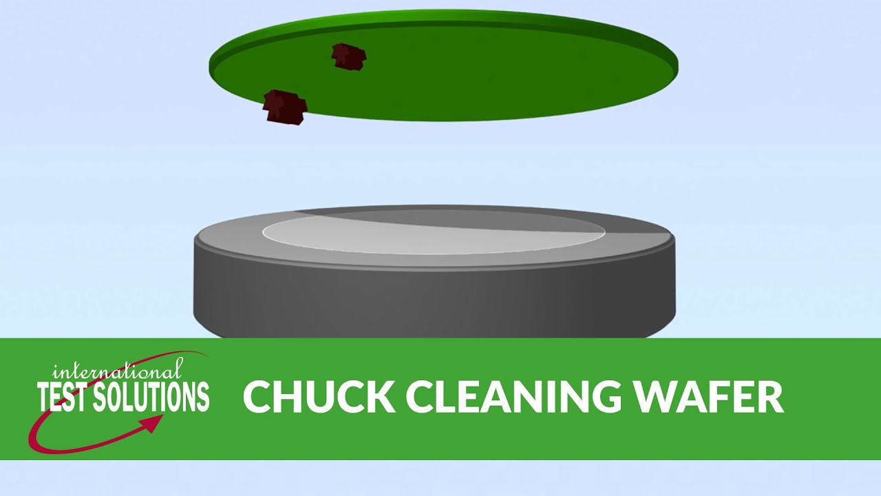
Plasma Etch tools are critical systems in the semiconductor device manufacturing process. The etch chambers require regular manual cleaning at scheduled intervals. Sometimes contamination on the wafer chuck can require cleaning prior to the scheduled time.
The Chuck Cleaning Wafer, or CCW, from International Test Solutions is an innovative turn-key product for efficient chuck cleaning without unscheduled downtime.
Learn more at https://www.inttest.net
electrostatic chuck semiconductor 주제에 대한 자세한 내용은 여기를 참조하세요.
The Electrostatic Semiconductor Wafer Clamping/Chucking …
The electrostatic chuck (ESC) is used in a variety of semiconductor processes to hold the wafer during processing. ESCs employ a platen with integral …
Source: www.advancedenergy.com
Date Published: 1/1/2021
View: 2440
Electrostatic chuck | Application – Matsusada Precision
An electrostatic chuck (E-Chuck, ESC) is a chuck that absorbs and fixes (chucks) a workpiece by using an electrical force that causes objects to attract each …
Source: www.matsusada.com
Date Published: 3/19/2022
View: 8345
What is an electrostatic chuck? – クリエイティブテクノロジー
Electrostatic chuck (ESC) is a specialized type of clamp used to hold down or pick up objects by electrical force, by attraction forces from static electricity.
Source: creative-technology.co.jp
Date Published: 6/18/2021
View: 734
Electrostatic Chucks | Chucks | USD – Entegris
We design and manufacture high performance electrostatic chuck solutions for advanced semiconductor processes. See specifications.
Source: www.entegris.com
Date Published: 3/13/2021
View: 3163
Ceramic Electrostatic Chuck | Services | SHINKO ELECTRIC …
SHINKO designs ceramic electrostatic chucks which are wely used for semiconductor wafer processing such as etching and CVD equipment.
Source: www.shinko.co.jp
Date Published: 8/23/2022
View: 6679
Electrostatic chucks | Products | NGK INSULATORS, LTD.
These electrostatic chucks are designed to chuck the silicon wafer and keep it flat, allowing the wafer to uniformly dissipate the heat received from the …
Source: www.ngk-insulators.com
Date Published: 10/21/2021
View: 1103
주제와 관련된 이미지 electrostatic chuck semiconductor
주제와 관련된 더 많은 사진을 참조하십시오 Chuck Cleaning Wafer: Etch Clean by International Test Solutions. 댓글에서 더 많은 관련 이미지를 보거나 필요한 경우 더 많은 관련 기사를 볼 수 있습니다.
주제에 대한 기사 평가 electrostatic chuck semiconductor
- Author: International Test Solutions
- Views: 조회수 4,176회
- Likes: 좋아요 17개
- Date Published: 2020. 5. 7.
- Video Url link: https://www.youtube.com/watch?v=ZL9ECO4MvJ4
What is an electrostatic chuck?
The electrostatic chuck (ESC) is used in a variety of semiconductor processes to hold the wafer during processing. ESCs employ a platen with integral electrodes which are biased with high voltage to establish an electrostatic holding force between the platen and wafer, thereby “chucking” the wafer.
What is wafer chuck?
Wafer chucks are used to hold wafers & die in place whilst they are being probed. Chucks can either use a mechanical clamp to hold the wafer in place, or apply a small vacuum from the backside of the wafer. The vacuum wafer chuck is the preferred option in most applications.
Probe Station Chucks Explained
It is standard practice for the chuck to be customised to the application, and so there are a great many types of chuck available to the operator when configuring their probe station. Examples include:
Most wafer chucks are made from aluminium and have nickel or gold plating, but some are manufactured from steel should the application require it. They will typically have flatness specifications that range from ±4 µm to ± 8µm.
Chucks come in a variety of sizes, materials and shapes depending on the wafer or die to be probed. Typically they are slightly larger than the size of the wafer and have concentric circular vacuum rings to allow them to hold multiple sizes of substrate.
Wafer chucks are used to hold wafers & die in place whilst they are being probed. Chucks can either use a mechanical clamp to hold the wafer in place, or apply a small vacuum from the backside of the wafer. The vacuum wafer chuck is the preferred option in most applications.
Thermal chucks:
One very common requirement for chucks is the ability to heat or cool the substrate. This requires a thermal chuck, sometimes referred to as a “hot” chuck. Thermal chucks can cover a wide range of temperatures; a standard range is from ambient (room temperature) to 200°C. At higher temperatures such as 300 or 400 °C, the materials of the probe arms, platen and chuck adapters need to be considered carefully, to avoid exposing the operator to hot surfaces.
Thermal chucks with a cooling capability require a chiller and cooling fluid, as well as shielding from the ambient environment. A number of cooling fluids are available such as water, nitrogen, Galden or clean dry air (CDA).
Localised environmental chamber:
To shield a device from the ambient air and to be able to probe below the ambient temperature, a localised environmental chamber (LEC) is required. These are chambers which encompass the device under test and allow for the creation of a controlled frost-free, light-free and EMI-free environment. They must be designed to adapt and fit within the probe station and allow the manipulators and probe arms to move and test without restriction.
Double sided chucks:
Some applications require the device under test to be accessed from both the front and backside simultaneously. For these a double sided chuck is available. These chucks can be configured to have openings below to allow the wafer to be optically inspected, or to be contacted by a probe, as the test application demands.
High frequency chucks:
High frequency chucks are often manufactured to hold a wafer as well as two calibration substrates, or a calibration substrate and a contact substrate. They are provided with a vacuum manifold kit that provides independent vacuum control to three quadrants. These are designed to be used to test devices at high frequencies.
High power chucks:
These are designed specifically for use in high power probing systems. Voltages up to 3 kV or 10 kV with coaxial, triaxial or Kelvin connectors are typical. They are available in both ambient and thermal configurations.
Packaged part holders:
A variant from the standard flat chuck, a packaged part holder is a fixture that can hold packaged parts, substrates and printed circuit boards. They can also be used to hold wafer chucks, allowing a single system to perform testing of whole wafers and packaged parts.
Lift pin chucks:
Chucks with lift pins are used in fully automated solutions where the wafers are transferred by a robot arm. The lift pins allow for safe and repeatable material handling when raising the wafer off the chuck base. The pins can be mechanically, pneumatically or electrically driven to raise and lower the wafer or substrate.
MEMS chucks:
These are chucks which can be inclined in X or Y to allow probing of particular regions of the MEMS device, which cannot be easily accessed from above or below. They are also suitable for use within vacuum chambers.
Whatever the probing application or specific requirements of your testing needs, a chuck or custom solution will be available.
Electrostatic chuck
An electrostatic chuck (E-Chuck, ESC) is a chuck that absorbs and fixes (chucks) a workpiece by using an electrical force that causes objects to attract each other with static electricity. When positive and negative voltages are applied to the internal electrodes of the chuck while the workpiece is placed on the chuck, the electric charges in the workpiece move so that they are attracted to the internal electrodes. This generates a Coulomb force between the electrodes and the workpiece, and the workpiece is adsorbed to the chuck.
Electrostatic chucks can be divided into two types according to the difference of the chucking method: one is the Coulomb force type that uses insulating material as the dielectric. One is the Coulomb force type, which uses an insulating material as the dielectric, and the other is the Johnsen-rahbek force type, which is induced by a small current flowing in a small gap at the interface between the object and the dielectric, resulting in an electrostatic polarization.
Electrostatic chucks are suitable for gripping very delicate workpieces such as metal foils and films because they do not use physical constraints. Therefore, they are used for chucks to transport wafers in semiconductor manufacturing equipment.
Matsusada Precision handles high-voltage power supply equipment for electrostatic chucks. Whether it is an electrostatic chuck using the Coulomb force or the Johnsen-rahbek force, we have the lineup for both.
Electrostatic Chucks
Leveraging proprietary coating technologies and innovative manufacturing capabilities, our electrostatic chucks offer a very flat clamped wafer surface, uniform thermal properties, improved gas-cooling, superior plasma erosion resistance and ultra-low particle and metal generation. These advanced wafer contact surfaces are made of materials with tailorable electrical properties, have an optimal wafer contact area that improves overall performance and lifetime while minimizing contamination.
Low particle and metal generation
Fast clamping and de-clamping
Reliable wafer clamping consistency
Ceramic Electrostatic Chuck
Introduction
SHINKO designs ceramic electrostatic chucks which are widely used for semiconductor wafer processing such as etching and CVD equipment.
SHINKO offers high quality, low cost, short lead time and manufactures using consistent production processes such as firing and machining of ceramic, assembly and inspection.
SHINKO’s electrostatic chucks meets customers’ state-of-the-art needs.
Features
Material: Alumina ceramic (Coulomb force type and Johnsen-Rahbek effect type)
Dimension: Max size φ300 mm
Ceramic thickness: 0.8~10.0 mm
Operation temperature: -20 ~ +200 °C
Ceramic Surface: Available for grooving, embossing surface and optional surface roughness
Others: Heater type is supported
Structure
Applications
Electrostatic chucks
Overview
These electrostatic chucks are designed to chuck the silicon wafer and keep it flat, allowing the wafer to uniformly dissipate the heat received from the plasma. NGK’s electrostatic chucks have excellent strength, thermal conductivity and thermal shock resistance and are capable for a wide range of temperature as a result of NGK’s proprietary volume resistivity control technology. NGK has aluminum nitride (AlN) and aluminium oxide (Al 2 O 3 ) materials for this application.
Advantages
Wide operating temperature range (-50~700 deg.C)
These electrostatic chucks have excellent strength, thermal conductivity and thermal shock resistance and are capable for a wide range of temperature by NGK’s proprietary volume resistivity control of ceramics.
High corrosion resistance
These electrostatic chucks have superior corrosion resistance against halogen gas.
Low particle treatment
Low particle treatment is available by surface treatment and special cleaning
High purity
Purity of 99.9% or higher is also available.
Heating function
The high-precision heating element embedding technology enables integration with the heater function, and the wafer temperature can be controlled to less than ± 1%.
Cooling function
These electrostatic chucks have extremely high cooling performance by bonding ceramic plate, which has high thermal conductivity, and a cooling plate.
RF electrode
Bulk metal electrodes provide stable wafer chucking and RF plasma generation at the same time.
Specification
Size Compatible with 200, 300 and 450mm wafer Chucking mechanism Johnsen-Rahbek (AlN), Coulomb (Al 2 O 3 ) Electrode shape Mono polar / Bi polar
AlN material properties
키워드에 대한 정보 electrostatic chuck semiconductor
다음은 Bing에서 electrostatic chuck semiconductor 주제에 대한 검색 결과입니다. 필요한 경우 더 읽을 수 있습니다.
이 기사는 인터넷의 다양한 출처에서 편집되었습니다. 이 기사가 유용했기를 바랍니다. 이 기사가 유용하다고 생각되면 공유하십시오. 매우 감사합니다!
사람들이 주제에 대해 자주 검색하는 키워드 Chuck Cleaning Wafer: Etch Clean by International Test Solutions
- 동영상
- 공유
- 카메라폰
- 동영상폰
- 무료
- 올리기
Chuck #Cleaning #Wafer: #Etch #Clean #by #International #Test #Solutions
YouTube에서 electrostatic chuck semiconductor 주제의 다른 동영상 보기
주제에 대한 기사를 시청해 주셔서 감사합니다 Chuck Cleaning Wafer: Etch Clean by International Test Solutions | electrostatic chuck semiconductor, 이 기사가 유용하다고 생각되면 공유하십시오, 매우 감사합니다.